
Breakthrough In Quantum Microscopy: Researchers Are Making Electrons Visible In Slow Motion
Eddie Gonzales Jr. – MessageToEagle.com – Physicists at the University of Stuttgart, led by Prof. Sebastian Loth, are developing quantum microscopy to record electron movement at the atomic level with unprecedented spatial and temporal resolution.

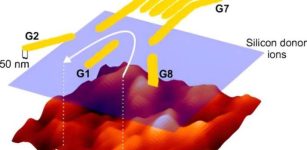
The imaging tip of the time-resolving scanning tunneling microscope captures the collective electron motion in materials through ultrafast terahertz pulses. Credit: Shaoxiang Sheng, University of Stuttgart (FMQ)
Their method has the potential to enable scientists to develop materials in a much more targeted way than before.
Prof. Loth, Managing Director of Stuttgart University’s Institute for Functional Matter and Quantum Technologies, states in a press release: “Our new method reveals previously unseen phenomena, allowing us to answer longstanding questions about electron movement in solids dating back to the 1980s.”
The findings of Loth’s group are also of very practical significance for the development of new materials.
Tiny changes with macroscopic consequences
Atomic-level changes in metals, insulators, and semiconductors typically don’t affect their macroscopic properties. Altered metals remain conductive, while insulators stay non-conductive.
In advanced lab-created materials, minor atomic changes cause new macroscopic behaviors. For example, some materials can abruptly switch from insulators to superconductors, conducting electricity without heat loss.
These changes occur within picoseconds, directly influencing electron movement at the atomic scale.
A picosecond, just a trillionth of a second, is to the blink of an eye what a blink is to over 3, 000 years.
Recording the movement of the electron collective
Loth’s team discovered a method to observe atomic-level changes in materials. They studied a niobium-selenium compound, focusing on the collective electron motion in a charge density wave.
Loth’s team studied how one impurity can halt collective movement. They applied a brief electrical pulse to the material, pressing the charge density wave against the impurity. This creates nanometer-sized distortions in the electron collective, causing complex electron motion for a short period.
Developing materials with desired properties
“Understanding how electron movement is halted can help us develop materials with specific properties,” Loth explains. This microscopy method helps determine how impurities should be arranged to achieve desired technical effects, as no material is perfect.
“Atomic-level design directly affects a material’s macroscopic properties,” Loth explains. This could be applied in ultra-fast switching materials for future sensors or electronics.
An experiment repeated 41 million times per second
“There are established methods for visualizing individual atoms or their movements,” explains Loth. “But with these methods, you can either achieve a high spatial resolution or a high temporal resolution.”
The laboratory setup requires exceptional shielding to measure weak signals accurately. Vibrations, noise, air movement, and fluctuations in temperature and humidity can interfere with measurements. Loth explains, “We measure extremely weak signals that are easily lost in background noise.” Multiple measurements are necessary to obtain meaningful results.
The researchers optimized their microscope to repeat the experiment 41 million times per second, achieving exceptional signal quality. Loth claims, “We’re the only ones who’ve accomplished this.”
The researchers have published their findings in Nature Physics.
Written by Eddie Gonzales Jr. – MessageToEagle.com Staff Writer
Related Posts
-
 Physicists Make Leaps In Reading Out Qubits With Laser Light
-
 More Stable States Of Quantum Computers – KIT Researchers Work On New Qubit Approach
-
 Continuous Time Crystal Observed By Researchers
-
 ‘Crazy’ Light Emitters: Unusual Quantum Phenomenon Observed
-
 SU(N) Matter Is About 3 Billion Times Colder Than Deep Space
-
 Quantum Teleportation: The Express Lane For Quantum Data Traffic
-
 Researchers Reach Quantum Networking Milestone In Real-World Environment
-
 Quantum Technology Could Make Charging Electric Cars As Fast As Pumping Gas
-
 Machine Learning Used To Bridge The Reality Gap In Quantum Devices – New Study
-
 Twisting Up Atoms Through Space And Time